1. If the length of a cylindrical conducting wire is doubled and area of cross section is halved the resistance of the wire becomes.
1) Double
2) Half
3) 4 times
4) 1/4 times
2. The average value of the full wave rectified sine wave with period m and a peak value of 1V is
1) 1.274V
2) 0.637V
3) 0.3185V
4) 1V
3. If the voltage applied across a capacitor is triangular in waveform, then the waveform of current flowing through the capacitor is
1) Triangular
2) Zero
3) Sinusoidal
4) Rectangular
4. An amplifier has a gain of (2/3) Ao, and produces a phase shift of 60°.Three of such amplifiers are cascaded. A feedback with feedback factor β=0.027 is applied to the cascaded system. Find the value of Ao required for the cascading system to become oscillatory.
1)5
2)-5
3) 0.66
4)-0.66
5. Two lamps X and Y are connected in series. The lamp X glows less bright than Y. Then
1) the resistance of X is greater than the resistance of Y
2) the resistance of X is lesser than the resistance of Y
3) the resistance of X is equal to the resistance of Y
4) there is no correlation between the resistances of X and Y
6. For a Common Source (CS) MOSFET amplifier, what is the input capacitance Cin for the following conditions Cgs=4pF, Cgd=1pF, and Av = 5
1) 10 pF
2) 16 PF
3) 14 pF
4) 12 pF
7. To design a low pass RC circuit with cut-off frequency of 500Hz and C=0.1uf the value of resistor required is
1) 3.184 Kohm
2) 0.318 Kohm
3) 10 Kohm
4) 1 Kohm
8. Decimal 43 in Hexadecimal and BCD number system is respectively
1) B2, 0100 0011
2) 2B, 0100 0011
3) 2B, 0011 0100
4) B2, 0100 0100
9. Pipelining method involves following steps to be run in parallel during instruction execution
1) Fetch, Decode, Execute and Write
2) Fetch and Execute only
3) Decode, Execute and Write only
4) Fetch and Decode only
10. To access a memory space of 32GB,________ number of address lines are required.
1) 32
2) 35
3) 34
4) 36
11. Complement of the expression A'B+CD' is
1) (A' +B)(C'+D)
2) (A+B')(C'+D)
3) (A'+B)(C'+D)
4) (A+B')(C+D')
12. Output of a 2-input AND gate is connected to one of the inputs of a multiple input OR gate. Which of the following statement is correct?
1) Output of the OR gate will always be 1
2) Output of OR will be same as output of AND gate
3) if any of the inputs of AND gate is one, the output of OR gate will always
4) If both the inputs of AND gate are 1, the output of OR gate will always be 1
13. In a Synchronous digital design, which of the following violations cannot be faced by changing the system clock time period?
1) Hold timing
2) Min Pulse Width
3) Setup timing
4) Transition violation
14. Number of 2:1 multiplexers required to implement a 5:1 multiplexer is
1) 4
2) 5
3) 3
4) 8
15. Initial state of MOD-16 down counter is 0101. After 40 clock cycles the state of the counter is
1) 1101
2) 1111
3) 0101
4) 1010
16. Which gate is used to check equality of numbers?
1) AND
2) OR
3) NOR
4) XNOR
17. Which one of the followings is non-maskable Interrupt in 8085 microprocessor.
1) INTR
2) TRAP
3) RST7
4) RST5.5
18. Decimal equivalent of unsigned binary number 10101011.1001 is
1) 171.5625
2) 171.5624
3) 171.5
4) 172
19. When can one logic gate drive many other logic gates in Digital Electronics?
1) When its output impedance is low and the input impedance is low
2) When its output impedance is high and the input impedance is high
3) When its output impedance is high and the input impedance is low
4) When its output impedance is low and the input impedance is high
20. Difference between a demultiplexer and a decoder is
1) None
2) decoder has one data input whereas demultiplexer has none
3) decoder has no data input whereas demultiplexer has one
4) decoder requires one additional control input than equivalent demultiplexer
21. To realize a 3-input XOR gate with only 2-input NAND gates, minimum count of gates required would be
1) 10
2) 8
3) 9
4) 6
22. In the circuit shown in the figure below, find the emitter current of the transistor, Consider op-amp is ideal and ꞵ of transistor 150.
1) 0
2) 1 mA
3) 5 mA
4) 0.65 mA
23. Which of the following graph represents the variation of resistivity (p) with temperature (T) for copper?
1)
2)
3)
4)
24. Find the current supplied by the source in figure. The resistors are mounted in a cylindrical form.

1) 14/13 A
2) 2 A
3) 3 A
4) 1.75 A
25. Assume all transistor are in saturation and the small signal gain of the circuit is G. Now the current of transistor M9 is increased to 4 times without changing size of any transistor What will be the value of gain after the increase in current?

1) 4*G
2) 2*G
3) G/2
26. Obtain the total power supplied by voltage source Vin=10V

1) 0 W
2) 1 W
3) 10 W
4) 100 W
27. Consider below simplified cross section of a CMOS device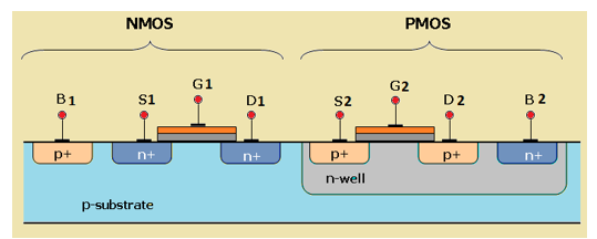
Which of the statement is true if this device is working as an inverter?
1) G1 and G2 are shorted, S1 and S2 are shorted, D1 and D2 are shorted
2) B1 and S1 are connected to ground and B2 and D2 are connected to power supply
3) B1 and B2 are connected to ground and S1 and D2 are connected to power supply
4) G1 and input and G2 is output of the inverter
28. Find the V out in following circuit if Threshold Voltage (Vt) of MOS=1V

1) 0V
2) 1V
3) 3V
4) 4V
5) 5V
29. The current I flowing through resistance 'r' in the circuit shown is

1) -V/12R
2) V/12R
3) V/6R
4) V/3R
30. In the circuit shown, choose the correct timing diagram of the output (y) from the given waveforms W1, W2, W3 and W4

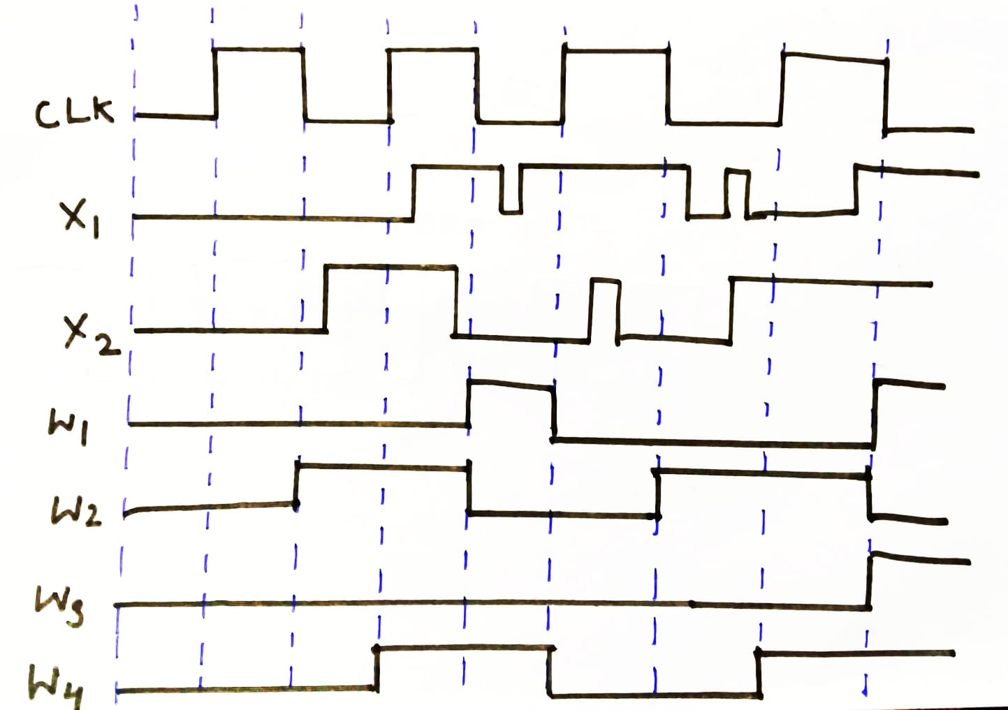
1) W1
2) W2
3) W3
4) W4
31. Mark the correct equation for hold time requirement at ff-capture in the shown diagram:
1) tclk-tsetup<thold+tcom + (2 x ta2z) + tck2q
2) tclk-tsetup <thold+tcom +(3 x ta2z) + tck2q
3) tck2q +tcom>thold
4) tck2q + tcom<thold
32. Which of the following assignments can convert S-R FF into a Toggle Switch (Output toggles with every clock pulse)?
1) S=R=Q'
2) R=S=Q
3) R=Q, S=Q'
4) S=Q, R=Q'
33. The following diagram is a representation of
1) Mod-8 counter
2) Mod-7 counter
3) Mod-6 counter
4) Mod-5 counter
34. In the following diagram the steady state frequency values at Dout1 , Dout2 and Dout3 would be
1) 0,0,0
2) 125 MHz,125 MHz,125 MHz
3) 25 MHz,12.5 MHz,6.25 MHz
4) 250 MHz,125 MHz,62.5 MHz
35. In the following diagram of frequency counter, the LED display shows count as 225(decimal) after one gate pulse (t=0.25 ms). What is the frequency of the input wave?
1) 100 Hz
2) 625 KHz
3) 225 KHz
4) 900 KHZ
36. Assume that N1 is in saturation region and I1 is ideal current source. What will be the impedance looking from source of N1?
1) 1/gm
2) 0
3) Infinite
4) Ro
0 comments:
Post a Comment